What is a 3nm chip? Nothing on it is 3 nm long
What a 3nm chip really is: "3 nm" is a generation name, and real transistor gates sit 48 nm apart. Why chips cannot shrink forever, and what AI needs next.
Mục lục
New phones advertise a “3 nm chip”, new laptops a “3 nm chip”, and next year it will be “2 nm”. It sounds as if engineers can now make features only 3 billionths of a metre across. The truth is more surprising: what is a 3 nm chip? It is the name of a technology generation, not a size. On a “3 nm” chip, nothing is 3 nm long. Two neighbouring transistor gates sit about 48 nm apart, and the gate itself is about 16 nm long[1]. The name and the real dimensions parted ways about twenty years ago.
This article explains why the number in a chip’s name is no longer a measurement, where physics blocks further shrinking, and why new chip generations matter so much for AI. The first half needs no electronics background. At the end there is a piece of code that plots the real dimensions of each chip generation.
A chip is billions of switches
The basic building block of every chip is the transistor, a tiny electrical switch: put a voltage on its “gate” and current flows, remove it and the switch turns off. On and off are 1 and 0, and every calculation, from adding two numbers to running an AI model, is built from billions of such flips.
The number of transistors on a chip today is hard to imagine. The A17 Pro chip in the iPhone 15 Pro, the first phone chip made with “3 nm” technology, has about 19 billion transistors. NVIDIA’s H100, the kind used to train large AI models, has 80 billion transistors[4].
Packing more switches into the same area means a chip can do more work, use less power per calculation, and cost less per transistor. That is why the whole industry has raced to shrink for sixty years.
When the number in the name was a real size
In 1965 Gordon Moore, later a co-founder of Intel, noticed that the number of components on a chip kept doubling at regular intervals, and predicted the trend would continue[5]. The observation became known as Moore’s law, and the semiconductor industry turned it into a work rhythm: every few years a new generation, called a node.
For decades the node name described a real size on the chip, close to the length of the transistor gate. A 1-micrometre node had gates about 1 micrometre long. Each new generation shrank every dimension by about 0.7, so the area of each transistor roughly halved.
Then, around 2000, as IEEE Spectrum put it, “physics started to get in the way of simply shrinking transistors”[2]. The industry kept releasing new generations and kept naming them on the old rhythm, but the number no longer matched any feature. By the “7 nm” generation, the transistor gate was about 15 nm long, twice the number in the name[2].
Why can chips not shrink forever?
There are three physical walls, and they went up at almost the same time.
The first wall: electrons pass through the barrier. The transistor gate is separated from the current below by an insulating layer. As things shrink, that layer gets thinner, until it is only a few atoms thick. At that thickness quantum mechanics starts to speak up: electrons can tunnel through the barrier even though, classically, they lack the energy to get over it, the same kind of effect mentioned in the article on quantum computers (article in Vietnamese). The switch no longer turns fully off, and leakage current keeps flowing, producing heat even when the transistor is doing nothing.
The second wall: heat. For decades, shrinking transistors also let voltage drop in proportion, so power density on the chip stayed roughly constant even as transistor counts soared. This rule is called Dennard scaling. The IRDS technology roadmap notes that it only held until before the 130 nm generation, in the early 2000s[1]. Since then voltage could not be lowered further because of leakage, and each new generation runs hotter per square millimetre. That is why CPU clock speeds have stayed at a few gigahertz for the past twenty years.
The third wall: atoms. The distance between two neighbouring silicon atoms is about 0.235 nm. A real “3 nm” feature would be only about 13 atoms long. The 12 nm gate length that the IRDS roadmap expects to be the final limit corresponds to about 50 atoms in a row. At that scale, a difference of just a few atoms makes two “identical” transistors behave differently.
How the industry got past the walls
Unable to shrink the old way, the industry turned to changing the shape and the materials of the transistor.
- New insulating materials. The traditional silicon dioxide layer was replaced by high-dielectric-constant (high-k) materials, thicker yet still in control, which block tunnelling current. Intel put them into production around 2007.
- Upright transistors (FinFET). Instead of lying flat, the channel stands up as a thin “fin”, and the gate wraps around three of its sides, controlling the current much more tightly. Since the early 2010s almost every high-end chip has used this design.
- Gate-all-around (GAA). The next step: the channel is a few thin sheets of silicon stacked on top of each other, and the gate surrounds all four sides of each sheet. On 30 June 2022 Samsung began producing “3 nm” chips with this kind of transistor, a first for the industry[3].
According to the IRDS roadmap, gate length will stop at about 12 nm and the distance between two gates will stop at 38 nm. After about 2031 there is no more room to shrink in the plane, and the way forward is stacking transistors on top of each other, like building upwards when you run out of land[1].
So what does “3 nm” measure?
If not a size, the number in the node name mostly says: this is a new generation, denser, faster or more power-efficient than the last. Each company names its own nodes, so one company’s “3 nm” is not necessarily another’s. The IRDS roadmap itself notes there is no agreement among manufacturers on how to name nodes[1].
As a replacement, the research group of Professor H.-S. Philip Wong (Stanford University) proposed in 2020 to measure density instead of size: how many logic transistors per square millimetre, how many memory cells, and how many connections between the processor and memory. Those three numbers go up as technology improves, instead of shrinking towards a meaningless number of nanometres[2]. The industry has not dropped the old names, because “2 nm” sells far better than “15% higher density”.
Why does AI need new chip generations?
Training a large AI model means performing enormous matrix multiplications, over and over, billions of billions of times. Two things decide its speed and cost: how much computing circuitry fits on one chip, and how much energy each operation takes.
New chip generations help with both. The H100 is built on a process from TSMC’s “4 nm” family, customised for NVIDIA, and holds 80 billion transistors on one chip[4]. Each following generation allows more compute circuits, more cache, or the same work with less power.
But the heat wall above does not go away. Since voltage cannot drop as it used to, more powerful AI chips usually also draw more power, and AI data centres are becoming huge electricity consumers, as analysed in the article AI does not just need chips (article in Vietnamese). That is also why people are exploring other paths, such as computing with light (article in Vietnamese) to move data with less energy.
Plot it yourself: node name versus real size
The Python below takes the numbers from Table MM-7 of the IRDS 2021 roadmap[1]: for each generation from “5 nm” (2021) to “0.7 nm” (expected 2034), the distance between two transistor gates, the distance between the two tightest metal lines, and the gate length. Then it puts them next to the number in the node name. You only need matplotlib.
import matplotlib.pyplot as plt
plt.rcParams.update({"figure.facecolor": "#16181c", "axes.facecolor": "#16181c", "text.color": "#d4d7dc",                     "axes.edgecolor": "#2a2e35", "xtick.color": "#878d97", "ytick.color": "#878d97", "font.size": 12})
# Table MM-7 of the IRDS 2021 roadmap (More Moore): node name and real dimensions, in nm.# gate: distance between two neighbouring transistor gates; metal: distance between the two tightest metal lines (M0);# length: gate length of a high-performance transistor.nodes = [    # year, node name, gate, metal, length    (2021, 5.0, 51, 30, 18),    (2022, 3.0, 48, 24, 16),    (2025, 2.1, 45, 20, 14),    (2028, 1.5, 42, 16, 12),    (2031, 1.0, 40, 16, 12),    (2034, 0.7, 38, 16, 12),]SI_BOND = 0.235  # distance between two neighbouring silicon atoms (nm)
print(f"{'year':>4} {'name':>7} {'gate pitch':>11} {'metal pitch':>12} {'gate length':>12} {'× node name':>12}")for year, name, gate, metal, length in nodes:    print(f"{year:>4} {name:>4} nm {gate:>8} nm {metal:>9} nm {length:>9} nm {gate / name:>11.0f}×")print(f"12 nm gate length ≈ {12 / SI_BOND:.0f} silicon atoms in a row; node name '3 nm' ≈ {3 / SI_BOND:.0f} atoms")
fig, ax = plt.subplots(figsize=(10, 5.2))xs = range(len(nodes))w = 0.26labels = [f"“{str(n).rstrip('0').rstrip('.')} nm”\n{y}" for y, n, *_ in nodes]ax.bar([x - w for x in xs], [g for *_, g, m, l in nodes], w, color="#8fa9c9", label="distance between two gates")ax.bar(list(xs), [m for *_, m, l in nodes], w, color="#a4a9b2", label="distance between two metal lines")ax.bar([x + w for x in xs], [l for *_, l in nodes], w, color="#e8b05a", label="gate length")ax.plot(list(xs), [n for _, n, *_ in nodes], "o-", color="#d4d7dc", lw=1.5, ms=7, label="number in the node name")ax.set_xticks(list(xs), labels)ax.set_ylabel("real dimension (nm)", color="#a4a9b2")ax.set_ylim(0, 58)ax.set_title("Node name versus real dimensions on the chip (IRDS 2021 roadmap)", color="#d4d7dc", fontsize=12)ax.grid(axis="y", color="#22262c")ax.set_axisbelow(True)  # grid behind the barsax.legend(frameon=False, labelcolor="#a4a9b2", fontsize=10, loc="upper right")fig.savefig("chip-3nm-kich-thuoc-that-en.png", dpi=150, bbox_inches="tight")
year name gate pitch metal pitch gate length × node name2021 5.0 nm 51 nm 30 nm 18 nm 10×2022 3.0 nm 48 nm 24 nm 16 nm 16×2025 2.1 nm 45 nm 20 nm 14 nm 21×2028 1.5 nm 42 nm 16 nm 12 nm 28×2031 1.0 nm 40 nm 16 nm 12 nm 40×2034 0.7 nm 38 nm 16 nm 12 nm 54×12 nm gate length ≈ 51 silicon atoms in a row; node name '3 nm' ≈ 13 atoms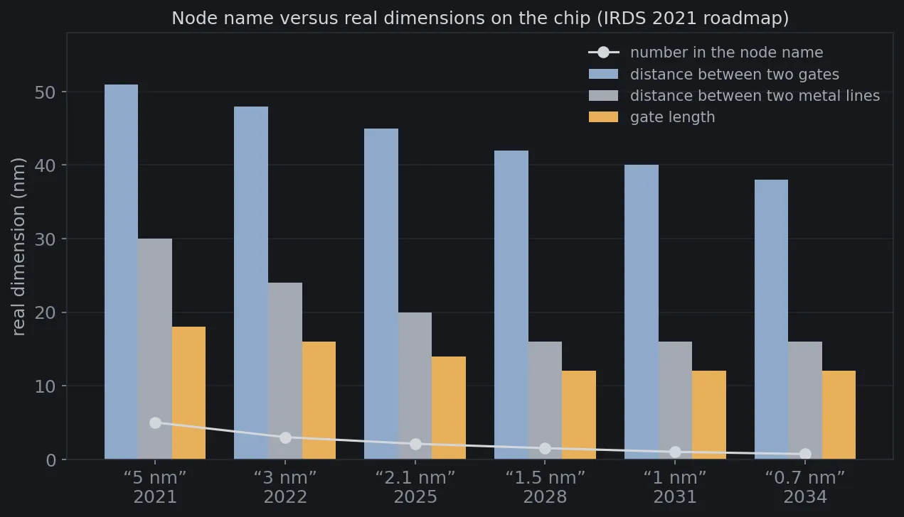
The last column of the table says it all: on a “3 nm” chip, the distance between two transistor gates is 16 times the number in the name. By the “0.7 nm” generation it will be 54 times. The names keep falling steadily out of habit, while the real dimensions are close to the floor, and further progress comes mainly from the shape of transistors and how they are stacked.
Shrinking in a different way
“3 nm” is not a lie, but it is not a size either. It is the name of a real step forward: denser, more power-efficient transistors, made in shapes that nobody mass-produced twenty years ago. It is just that the road no longer runs through making everything evenly smaller, but through quantum physics, materials science and three-dimensional architecture.
Next time you read about a “2 nm chip” or a “1.4 nm chip”, you will know: it is the name of a generation, and inside, the switches are still tens of nanometres wide, arranged ever more cleverly.
Free geometry illustrations for students and teachers: EyeViz.
Tài liệu tham khảo
- [1]International Roadmap for Devices and Systems (IRDS) 2021: More Moore, Table MM-7. IEEE, 2021.
- [2]Samuel K. Moore. Experts Invent a New Way to Track Semiconductor Technology. IEEE Spectrum (on the paper by H.-S. Philip Wong et al. in Proceedings of the IEEE), 2020.
- [3]Samsung Begins Chip Production Using 3nm Process Technology With GAA Architecture. Samsung Newsroom, 2022.
- [4]NVIDIA Hopper Architecture In-Depth. NVIDIA Technical Blog, 2022.
- [5]Gordon E. Moore. Cramming more components onto integrated circuits. Electronics, 38(8) (reprinted in IEEE Solid-State Circuits Society Newsletter, 2006), 1965.